What a logic gate IC does
A logic gate takes one or more digital inputs and produces a digital output. Its two logical states are usually called low and high, or 0 and 1. These names describe how a circuit interprets a voltage; they do not mean that every device uses the same voltage for a 1. A gate IC may contain several separate gates in one package, often sharing power and ground pins.
An AND gate outputs high only when all its inputs are high. An OR gate outputs high when at least one input is high. A NOT gate, also called an inverter, changes high to low and low to high. NAND and NOR gates invert the results of AND and OR. An XOR gate outputs high when its two inputs differ, making it useful for detecting a change or disagreement between signals. The corresponding XNOR gate outputs high when they match.
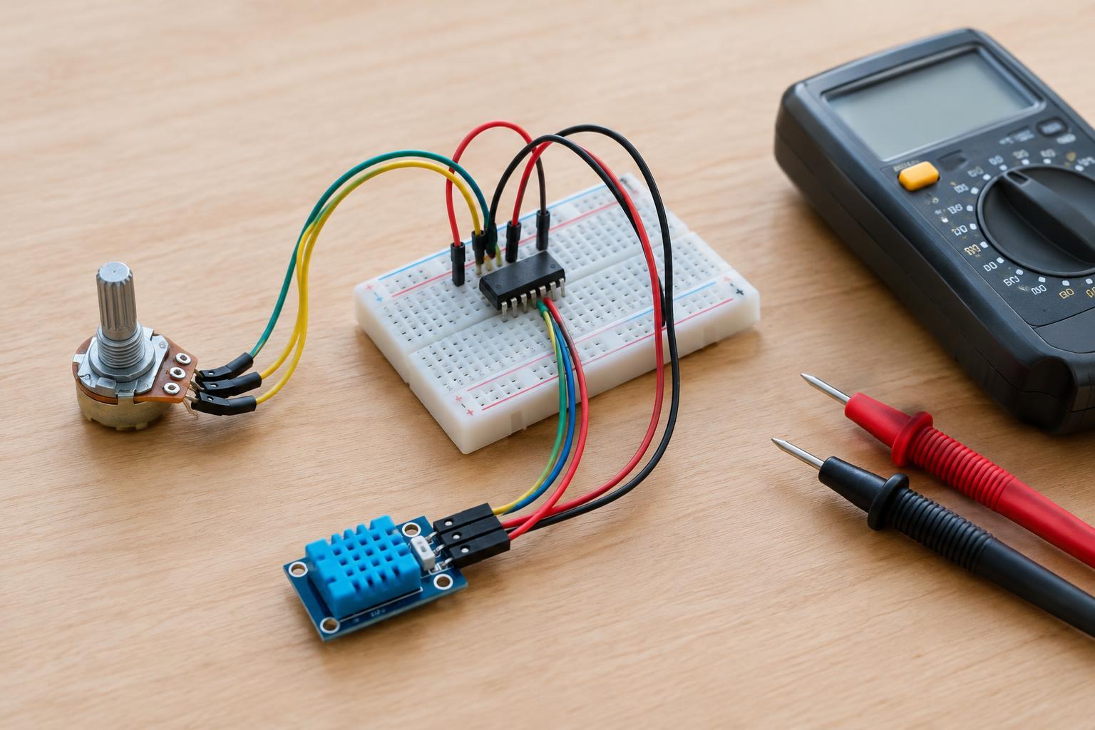
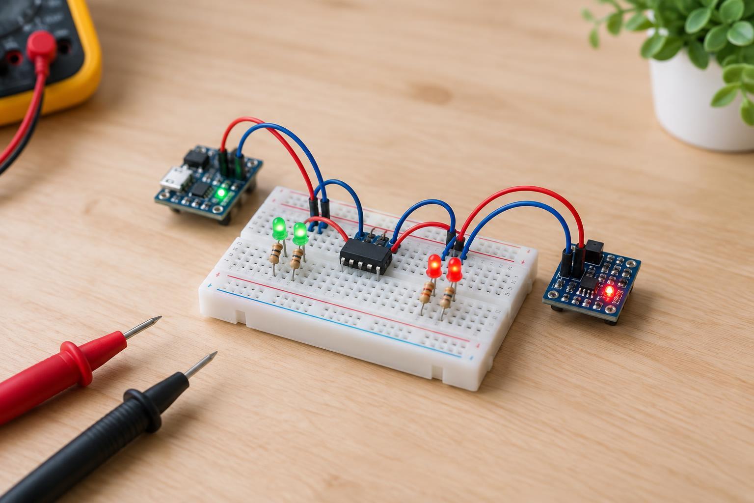
These functions can combine switches, sensor outputs and other digital signals without a microcontroller. For example, an AND gate can require two conditions before enabling a low-voltage indicator circuit. The logical rule is only part of the design, though: the signals must also be electrically compatible.
Logic states depend on voltage thresholds
A gate recognizes an input as low below a specified input-low limit, usually written VIL, and as high above an input-high limit, VIH. Between those limits, its behavior may not be reliably defined. Its output specifications describe how high it can guarantee a high output, VOH, and how low it can guarantee a low output, VOL, under stated conditions.
To check a proposed connection, compare the driving device’s guaranteed VOH with the receiving device’s required VIH. Then compare the driver’s guaranteed VOL with the receiver’s required VIL. Leave room for variation rather than relying on typical values alone. The guarantees may change with supply voltage and output load, so use the conditions that match your circuit.
Supply voltage is a separate specification. A device powered at 3.3 V is not automatically able to accept a 5 V input, even if it can recognize that input as high. Check its permitted input-voltage range and whether the particular pin is rated as 5 V tolerant. Likewise, a 3.3 V output may or may not meet the high-input requirement of a gate powered at 5 V. The data sheets for both parts settle the question.
Choose a family, not just a gate symbol
Parts with the same gate function can have different electrical characteristics. For example, 74HC and 74HCT devices may both provide a NAND gate, but their input thresholds are not interchangeable. At an appropriate 5 V supply, an HCT input is designed for TTL-compatible logic levels; an HC input generally follows CMOS-style thresholds tied more closely to its supply. Neither label alone tells you that a particular part accepts every voltage you might connect to it.
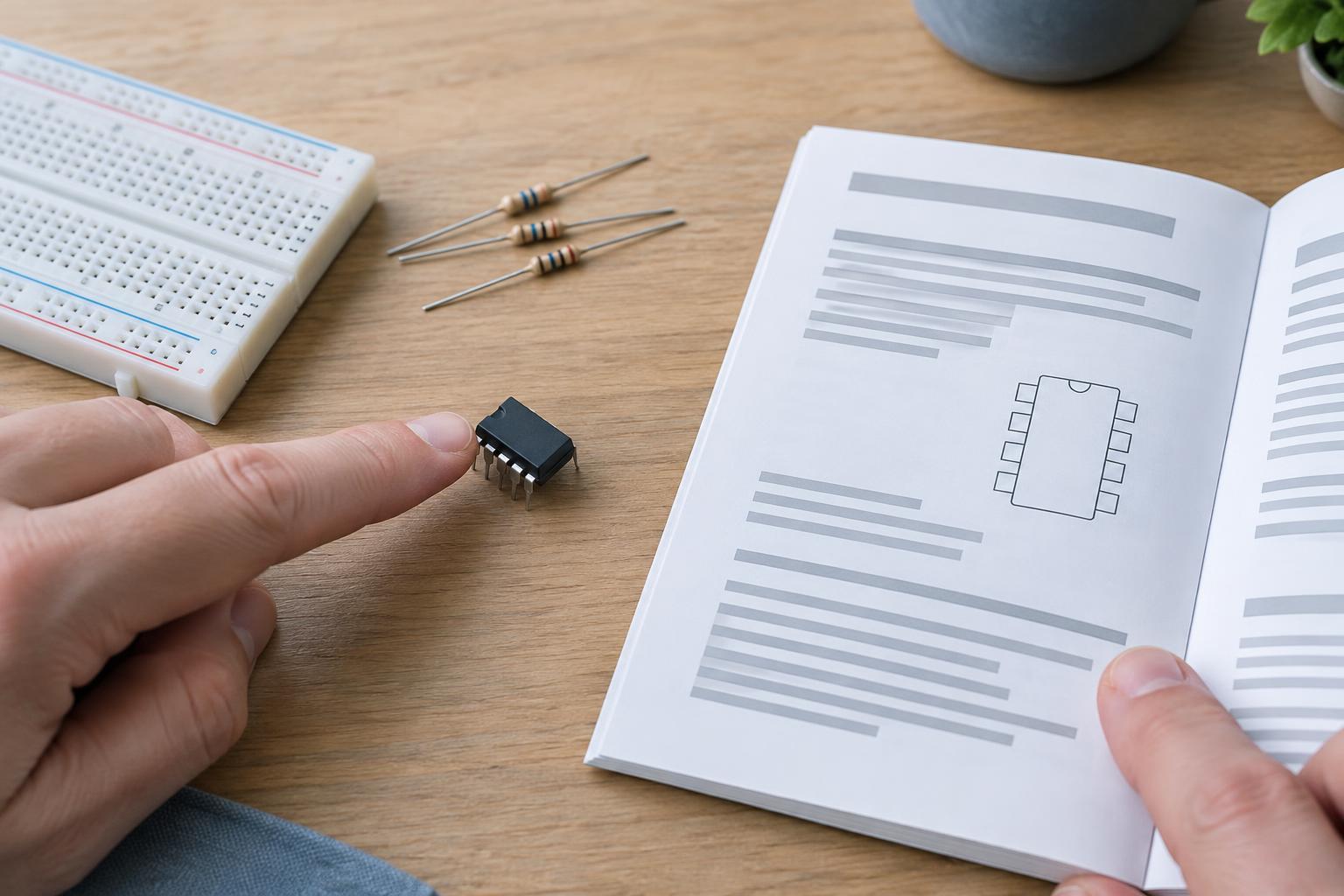
Other families, including members labeled LVC, can offer different supply ranges and input features. Capabilities can vary by exact device and manufacturer. Before substituting one IC for another, check the full part number, its recommended operating conditions, input limits, output-drive specifications and pinout. Absolute maximum ratings describe boundaries to avoid, not targets for normal operation.
Also consider what the output must drive. A logic gate is intended to signal other circuitry, not necessarily to power a motor, relay or a large collection of LEDs. If the load exceeds the gate’s specified drive capability, use a suitable driver stage instead.
Connecting gates safely in a low-voltage project
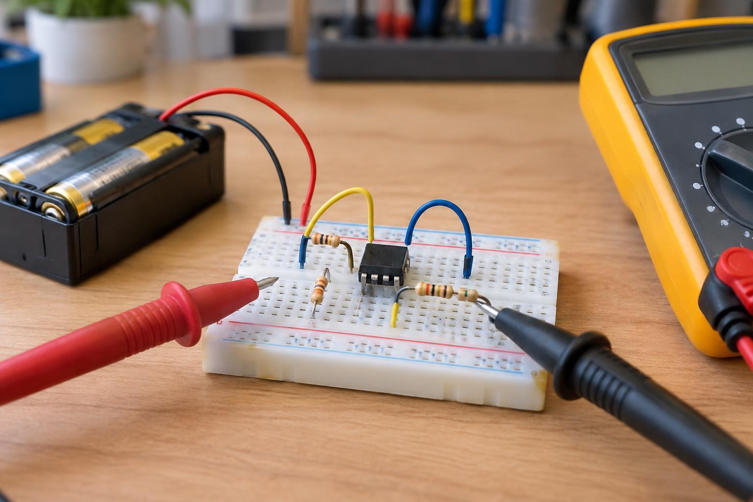
For a first breadboard test, use a regulated low-voltage supply within the IC’s recommended range and connect its ground to the ground of any device exchanging signals with it. Follow the package pinout rather than assuming power pins occupy familiar positions. A small ceramic bypass capacitor placed near the IC’s power pins is commonly recommended; check the part’s documentation for its requirements.
Do not leave ordinary CMOS gate inputs floating. An unconnected input can pick up noise and switch unpredictably. Connect unused inputs to a valid high or low level as appropriate for the device and your circuit, while avoiding shorts between outputs. A push-pull output should not be tied directly to another push-pull output unless the design explicitly permits it.
When two voltage domains do not meet each other’s input requirements, use an appropriate level-shifting circuit or a compatible intermediary device. Some open-drain or open-collector outputs can use a pull-up to a suitable receiving voltage, but only if the output pin and both devices’ operating conditions allow it. Check behavior when one device is unpowered, too: a signal applied to an unpowered IC can sometimes feed current through its input protection circuitry.
A quick compatibility checklist
Before wiring two digital parts together, identify each exact part and its supply voltage. Find the receiving pin’s VIL, VIH and allowed input range; find the driving pin’s VOL, VOH and output-current limits. Verify that the guaranteed output levels satisfy the input thresholds at the intended load. Confirm shared ground, correct pin assignments and a safe plan for unused inputs and power-up conditions.
This check separates two questions that are easy to confuse: “Will the receiver understand the signal?” and “Can the receiver tolerate the signal?” Both answers must be yes. Once the electrical interface is sound, the gate’s truth table becomes a straightforward way to predict what the circuit will do.